Power Integrations LinkSwitch-II CV/CC Switchers
Power Integrations LinkSwitch®-II family of CV/CC switchers simplify low power CV/CC charger designs by incorporating a 700V power MOSFET, a novel On/Off control state machine, and other features onto a monolithic IC. The devices include a revolutionary control technique that provides tight output voltage and current regulation, as well as compensates for transformer and internal parameter tolerances and input voltage variations. The product requires no optocoupler or secondary CV/CC control circuitry and eliminates the control loop compensation circuitry.Features
- Compensates for
- Transformer inductance tolerances
- Input line voltage variations
- Cable voltage drop (LNK61X series)
- External component temperature variations
- Very tight IC parameter tolerances using proprietary trimming technology
- Frequency jittering greatly reduces EMI filter cost
- Even tighter output tolerances achievable with external resistor selection/trimming
- Up to 85kHz programmable switching frequency to reduce transformer size
- Auto-restart protection reduces the power delivered by > 95% for output short-circuit and control loop faults
- Hysteretic thermal shutdown (automatic recovery reduces power supply returns from the field)
- Meets high-voltage creepage requirements between DRAIN and all other pins both on the PCB and at the package
Applications
- Chargers for cell/cordless phones
- PDAs
- MP3/portable audio devices
- Adapters
- LED drivers
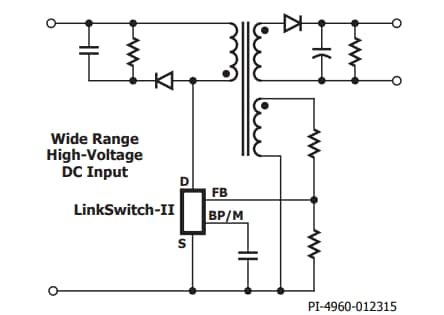
Application Circuit

Published: 2008-07-30
| Updated: 2022-03-11


